When it comes to implementing an RF design often it is good enough to use the layout example provided by the manufacture’s evaluation PCB design. But, sometimes we may want to create a more compact layout or perhaps use different component sizes or values. This is when it becomes beneficial to use a good EM tool for modeling parasitic properties of a substrate.
In this analysis below I show how to estimate the impedance of the bluetooth output of the Nordic Semiconductor’s nRF52840 chip using Sonnet Software – a 2.5D EM analysis tool.
Nordic Semiconductor provides a link to download the Altium Design files for their evaluation boards that use the nRF52840-CKAA chip. This example uses the following Altium project (follow the link to download the Altium project files):
nrf52840_ckaa_var1.PrjPCB
https://www.nordicsemi.com/Products/nRF52840/Compatible-downloads#infotabs
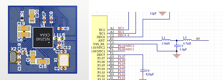
The bluetooth output of the nRF52840 is connected to a matching T network consisting of three components, L1, C3 and L5.
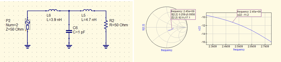
Without using an EM analysis tool we get the following impedance.
The (incorrect) impedance presented to the nRF52840 is 82.6 – j17.1 ohms or 82.6 ohms in series with 3.8pF. The conjugate impedance is the 82.6+j17.1 ohms or 82.6 ohms in series with a 1.1nH inductance.
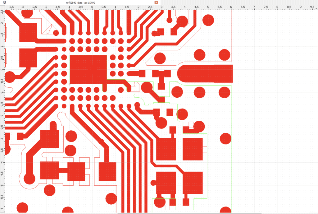
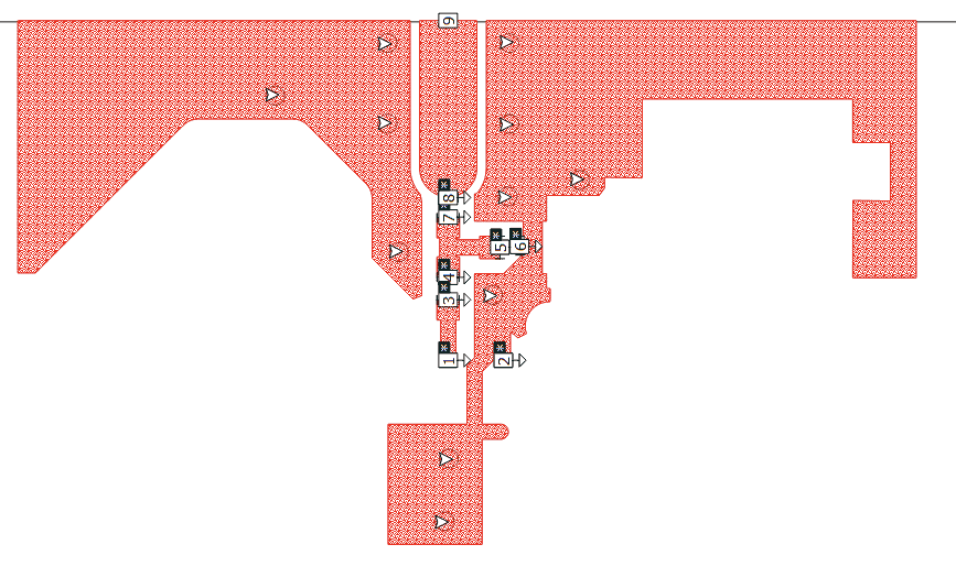
The layout was exported from Altium to a DXF (shown below) and this was later imported into Sonnet after cleaning up the DXF.
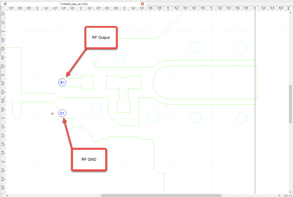
Below shows the cleaned DXF that was used imported into Sonnet. This intermediate step will lower simulation memory requirements and time it takes for the simulation to finish. The RF output of the nRF52840 are marked in the screen capture below – balls/pins E1 is the RF output. C1is the RF ground reference.
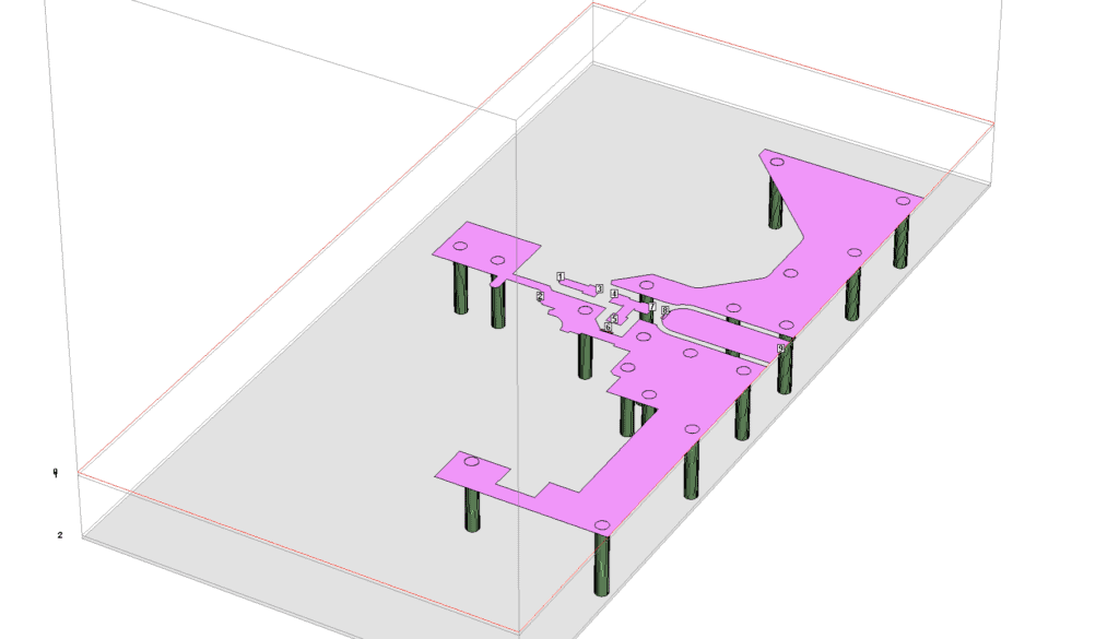
Blow is the sonnet model with 9 ports. Ports 1 & 2 connect to the RF output of the nRF52840. Port 9 is the output of the evaluation board (where the RF connector attaches at the end of the PCB). All of the other ports are for the LC T network.
Sonnet can display a model in 3D. This can be convenient while building a model. The top layer metal is displayed in purple, the vias are displaced in a dark green color. The Z-direction is scaled differently making the substrate appear thicker relative to the dimensions of the x-y plane.
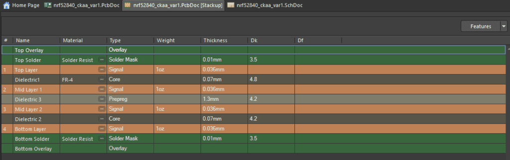
Stackup information was gotten from the Altium Design files
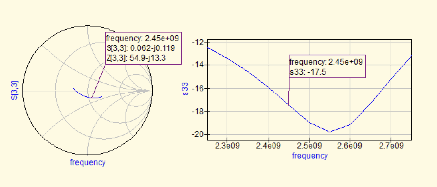
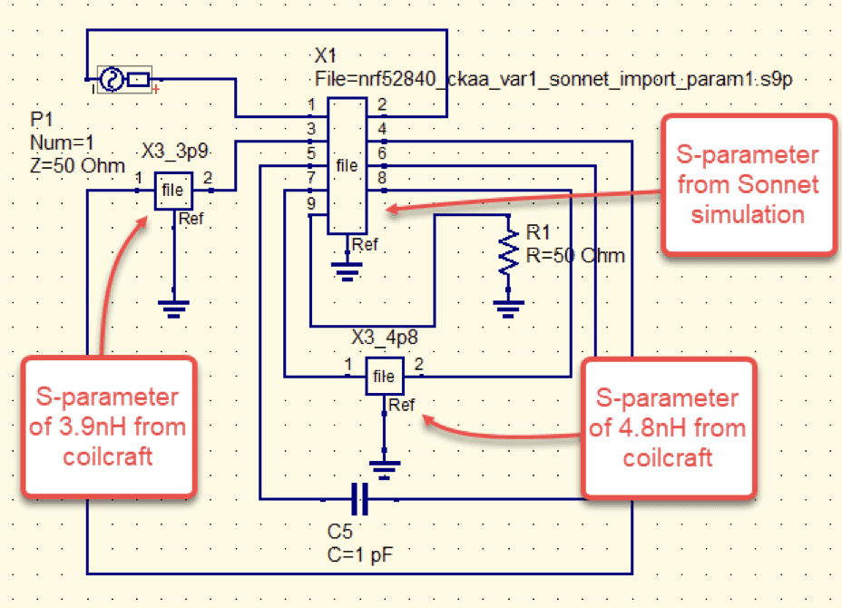
After creating the Sonnet model and running the simulation – an s-parameter file was then exported from Sonnet and into a linear circuit simulator. QUCS was used to simulate the data exported from Sonnet along with ideal inductances and capacitances.
Already we see a big difference in this simulation. Impedance presented to the nRF52840 is 54.9-j13.3 ohms or 54.9 ohms in series with 4.9pF. The conjugate impedance is 54.9+j13.3ohms or 54.9 ohms in series with a 0.86nH inductance.
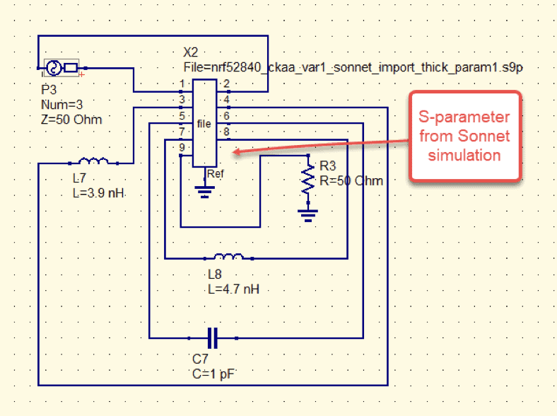
Taking this a step further we can model the inductances using data provided by Coil Craft. From the Coil Craft website the s-parameters for the 3.3nH and 4.8nH inductors were imported into QUCS.
Now we get a better picture of how the network transforms the impedance of the nRF52840 chip. Impedance presented to the nRF52840: 48.6 -j12.3 ohms or a series resistance of 48.6 ohms with a series 5.28pF capacitance. The conjugate impedance is 48.6 + j12.3 or 48.6 ohms with a series 0.8nH inductance.
Summary
The bluetooth output impedance of the nRF52840 is fairly close to 50 ohms and slightly inductive.
nRF52840 Bluetooth Output Impedance
48.6 ohms with a series 0.8nH